Introduction
You only have to watch a few commercials while enjoying your favorite show to have a sense of the smart phone market today. Top tier smart phone manufacturer brands(OEMs) are in fierce competition for market share. The problem is, in a general sense, each company can produce a quality phone capable of the usual features — call, text, web browsing, etc. To differentiate and distinguish their products each brand is pushed to incorporate more and more cutting-edge technologies to showcase new features. The smartphone camera has been a particularly crucial component in this marathon of innovation. With each improved lens or new bit of optical technology, a company could claim better quality photos, dynamic images, improved lighting, movie quality video capabilities, and the list goes on. More than “just” your camera app, these same optical technologies began to transcend serving basic applications and have become a means to immerse and integrate a user within a wide variety of powerful experiences. A simple example is facial recognition, by giving people the ability to securely unlock their phones with just a flash of their face, they’ve made the smartphone just a bit more of an extension of our everyday lives.
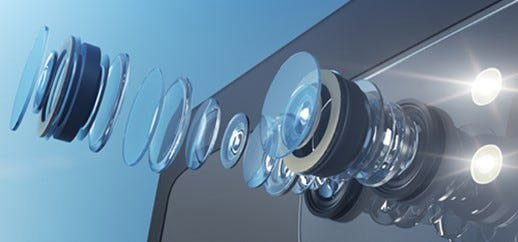
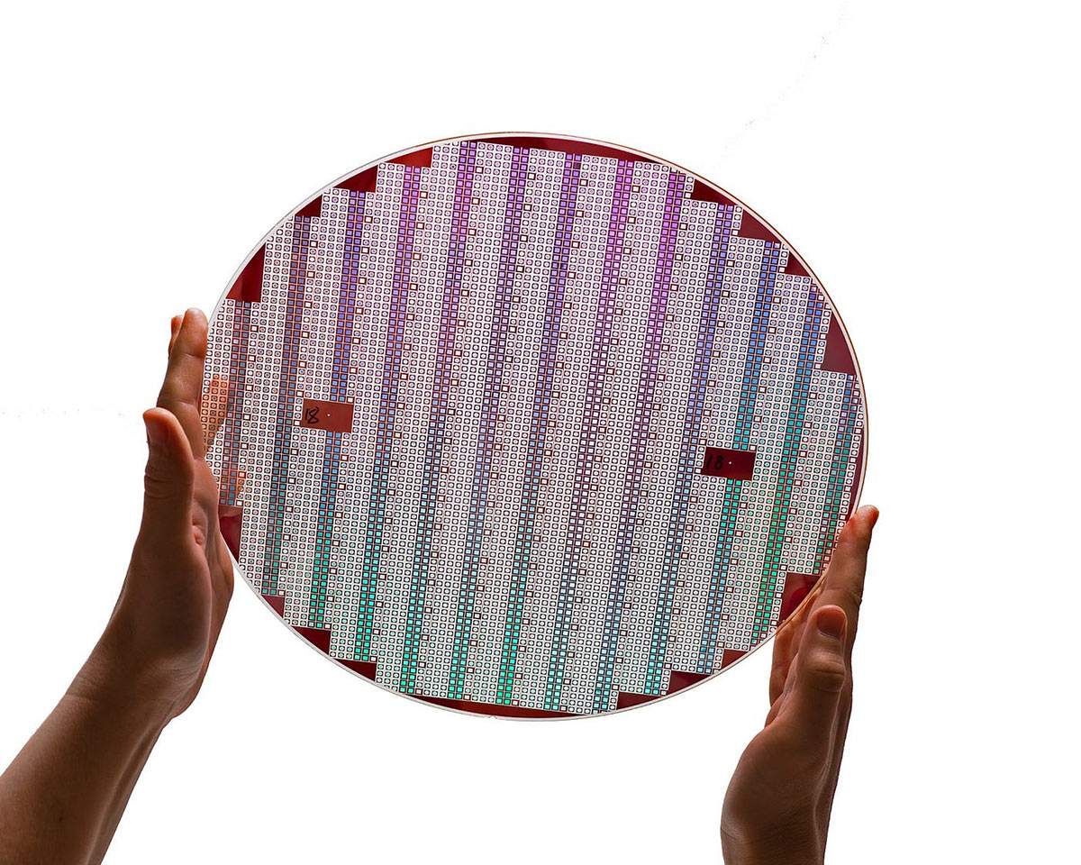
Figure 1
Figure 1. Consumer products like smart phones, are packed with intricate technology to enable differentiating capability — among the most critical being optical sensing tech. Image from Optical components and assemblies[1] .
While smartphones are a perfect case study, the true underlying conclusion here is just how important optical imaging technologies are. They have changed the way we bridge the gap between the physical world around us and the digital world we interact with daily. They are the gatekeepers of how we as people interact and immerse ourselves in various technology applications, more than just phones, and computers, they are everywhere — cars, security, banking, you name it. More than convenience they represent a substantially significant pathway to digital transformation.
Inherent to such an enabling technology, there is a persistent push for smaller, lighter, and simpler optical imaging and illumination components to drive ever more intricate innovations. For progress to continue, there is a need to rethink optical imaging sensors and illuminators to improve performance, increase efficiency, reduce cost, and usher in the next generation of optically reliant tech for more powerful applications.
Market Pains as Pathways to Progress
Having a firm understanding of the critical role optical sensing technologies play, was necessary before we at TDK Ventures could properly work to impact entrepreneurs and their developing technologies in the field. We had to develop a grounding in what current obstacles currently abated progress and what possible visions there were for the future.
Because optical imaging sensors are primarily driven by consumer products, so too are their design constraints and their price points. Relatively low price, easy manufacturability, and small size are key, and many state-of-the-art developments in optics and optical sensors are the opposite — high cost with complex manufacturing. To bring more to the table in their products, most OEMs need more tech in much less space. Any new innovations must be able to be highly efficient, capable of complex operations, cheap, and easy to produce at high yield — the silver bullet being one product that does all these things in one and replaces prior components that can then be removed.
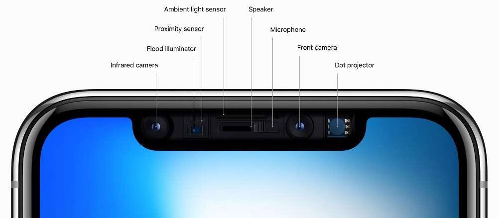
Figure 2
Figure 2. Camera and illumination components packed into the front face of a typical smart phone. Image from EE Times Asia[2].
Separate from manufacturing, volume, and complexity concerns (though inherently linked) are capabilities and performance — those magic factors which can differentiate a product in market — driven by the ever-competitive consumer products (e.g., smartphone) development. Today’s apps are pushing the boundaries on how much information can be extracted from an image. Consider for example apps that, using your picture, can give your clothing measurements, perform facial recognition, implement eye tracking, or perform analysis of your surrounding environment. The key is being able to extract three-dimensional positioning data (an object’s precise location in 3D space) from what we would ordinarily see as just a two-dimensional image. Using advanced optical imaging tech to determine the distance quickly and accurately between a camera and object in front of that camera unlocks literally another dimension of possibilities and so is currently an important driver in development. It is these types of capabilities that are fueling so much innovation in the booming AR/VR markets. Though, like within AR/VR, to do so often requires additional sensors, more parts, and more volume. A potential game changer in optical sensors is not necessarily technology that can do this, that is established, but tech that can do so in a simple — manufacturing friendly — way.
While our discussion here is not exhaustive, another critical concern is power draw. No one wants a phone that dies with just a few hours of usage. To maintain life, hardware must be designed to minimize power draw while still delivering on capabilities. In short, the industry needs optical tech that check all the boxes on manufacturing and cost, enable features that are on the forefront of technology, and use relatively low power — simple, right?
Metalenz: A Vision for the Future
Short answer — not simple. Technology that could deliver on such significant demands would be groundbreaking deep tech innovations firmly grounded in material science and optical expertise. It all comes down to leveraging light and how that light can be manipulated, and what information can be extracted. Fortunately, the world class team at semiconductor optics startup Metalenz has found a way to provide the industry with an incredibly powerful and innovative solution.
Metalenz designs, manufactures, and sells metasurface optics (meta-optics) at high volumes to meet the needs of many industries including consumer electronics, automotive, and AR/VR. Their meta-optics are a paradigm shift in optical sensing technologies and we believe they are a game-changer. The key technology here of course is metasurface optics, but what exactly are meta-optics? To answer that, first let’s consider the current state of the art.
Consider the infrared camera, flood illuminator, and dot projectors on typical smart phones — responsible for facial recognition, eye detection, sending signals to other devices, image detection in low light, and other useful applications. These are all reliant on taking light from a point source (usually a very small and low power laser) and reliably distributing that light over a given area. This enables things like flood light to provide better imaging for a camera, or even determining the distance between the smart phone and an object in front of the camera (e.g., 3D facial recognition). To achieve this, light is traditionally transmitted through one of two different optical components:
1. Traditional glass or plastic lenses, which because of the manufacturing curvature of the lens and the chemical characteristics of the material, bend and manipulate light to one or more points, depending on how many are used and in what shape.
2. Diffractive optical elements (DOEs) where material is manufactured on a much smaller scale and can similarly refract light, albeit with tighter, more controllable specifications and without the need for bulky curvature.
Both represent a progression of the same technology, with refractive lenses being a seminal design and DOEs following as an improvement. Taking up a significantly smaller footprint, and with much more precise control over light manipulation — they have enabled the current generation of smart phones and camera size. However, both are governed by the same physical laws and are reliant on the limits of material chemistry and geometry. It is for this reason that they are also size limited, with refractive lens taking up on the order of 1–10 millimeters and requiring curvature.
Meta-optics are fundamentally different. They are planar surfaces consisting of incredibly tiny, nanoscale, structures of precision designed shape and geometry. When light passes through the surface, the structures manipulate light in a predictable way such that the light is then emitted according to specifically designed polarization, phase, amplitude, spectrum, and emitted in a particular diffuse pattern or angle. This approach can provide superior performance and control, and allows the meta-optics to take up significantly less space than traditional lenses or DOEs.
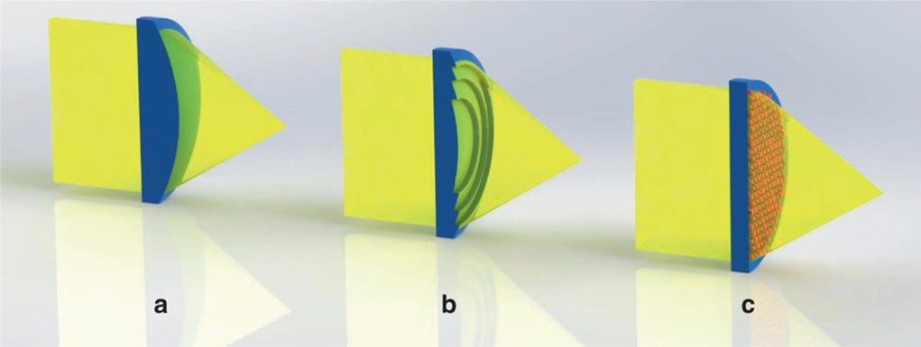
Figure 3
Figure 3. Illustrated comparison between (a) refractive lenses, (b) DOEs, and © meta-optic surfaces as published in Nature[3] .
Metalenz’ patented metasurface optics technology is able to achieve smaller, flatter, and lighter optics that have better performance, take up less space, and cost less to make than historical approaches. Surfaces can be readily manufactured at industry relevant volume and speed as they are fabricated using the same manufacturing processes used for CMOS chips and other semiconductors across the computer industry.
Metalenz technology can reduce a stack of four legacy refractive lenses that would traditionally be used in a smart phone camera to only one single flat metasurface optic. Similarly, Metalenz can reduce the multiple lenses required in illuminators, like dot pattern projectors, to just one single flat metasurface optic[4] . Performance includes inherent temperature stability, 2x better light collection, and 40% signal to noise reduction compared to other approaches.
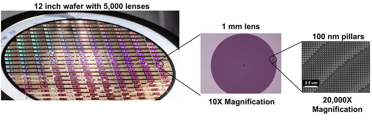
Figure 4
Figure 4. A Metalenz chip shown at different magnification highlight the size of the nanoscale structures that enable superior light manipulation. Image from TechCrunch[5]
Metalenz has quickly distinguished themselves as the global king of the hill innovator in optical technologies for mobile devices. Their groundbreaking metasurface optics have garnered fast attention of industry giants, and they have already partnered with the likes of Intel, Applied Materials, ST Micro, and others.
Spun out of a world-renowned research laboratory at Harvard, the company stands on several hundreds of patents established over decades in optics and metasurface development. Their founding leadership team, including Chairman Professor Federico Capasso and CEO Dr. Robert Devlin are world class technical experts with a deep understand of the technology and a passionate vision for its role in the industry moving forward. Quite simply there is no other company out there that can achieve the same performance, at the same cost and scale, with solid commercial traction, and that’s already in mass production.
Why We Invested
In exploring the technology area, the TDK Ventures team was quickly impressed by Metalenz. Their vision for the future, and their passion to make it a reality has backed by rigorous scientific experimentation and demonstration, and adeptly addressed a key market need in the world of optical technologies. From a market outlook standpoint, the global small device optical 3D sensing market represented a roughly 44% compound annual growth rate from 2017 to 2022 alone with no signs of slowing, and more specifically a greater than 74% CAGR in consumer apps — so an approximately $18 billion total addressable market. As part of these markets, there is significant alignment with TDK, including synergies with TDK across micro-actuators, AR/VR components, and optical image stabilization solutions.
Complementing the impressive ROI potential and partnering opportunities, we found deep alignment with Metalenz with respect to our core values and mission goals. At TDK Ventures, we aspire to be constantly mindful and supportive of global and responsible digital and environmental transformation. Naturally, we see Metalenz as having huge potential in driving digital transformation serving as an enabling technology in optics innovation for more than just smart phones, but to other small mobile devices, sensors for AR/VR, and robotics.
Utilizing Metalenz technology would also mean significant contributions to global sustainability due to their efficient and cost-effective manufacturing process. Achieving the production scale they have at the impressive price point and performance level could unlock the use of these components in other, potentially lifesaving industries. Their meta-optics can be used in medical devices like endoscopes and thus aid in the early detection of disease. Metalenz technology represents a brand-new approach to an old optical problem, using material science innovation to change the way we see the world.

TDK Ventures Team Members Visiting Metalenz
References
[1] Optical components and assemblies | Optical thickness Gauge applications. (2023, March 8). Bristol Instruments. https://www.bristol-inst.com/optical-components-and-assemblies/
[2] EETimes Asia. (2019, November). The Road to Smartphone Dominance. https://www.eetasia.com/the-road-to-smartphone-dominance/
[3] Engelberg, J., & Levy, U. (2020). The advantages of metalenses over diffractive lenses. Nature communications, 11(1), 1–4.
[4] Metalenz launches Orion™, the world’s simplest, most compact dot pattern projector. (2021, May 27). https://www.businesswire.com/news/home/20210527005558/en/Metalenz-Launches-Orion%E2%84%A2-the-World%E2%80%99s-Simplest-Most-Compact-Dot-Pattern-Projector/
[5] Coldewey, D. (2021, February 4). Metalenz reimagines the camera in 2D and raises $10M to ship it. TechCrunch. https://techcrunch.com/2021/02/04/metalenz-reimagines-the-camera-in-2d-and-raises-10m-to-ship-it/