Introduction
Henry Huang, Ph.D. Investment Director, TDK Ventures
Introduction: The Need for Innovation in Interconnections
More than 30 years ago, Dr. David Miller from AT&T Bell Labs succinctly encapsulated one of the greatest technical challenges that faces progress in our modern world Figure 1: “The performance of systems is determined much more by the interconnection than the speed of the devices themselves.”
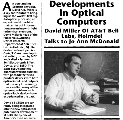
Figure 1. Dr. David Miller talked on Development in Optical Computer in 1990. 1
And indeed, his assertions have proven to be reality. It’s been over 60 years since the early rise of digital computers and when Moore’s law (“The speed and capability of computers can be expected to double every two years, as a result of increases in the number of transistors a microchip can contain”) took hold Figure 2. Processing capability has continued to skyrocket 2, all the while what connects our systems and allows data to move — network and memory bandwidth — has continued to lag and are falling further behind at an alarming rate 3 Figure 3.
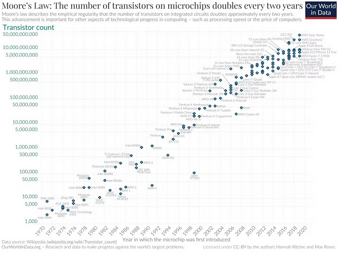
Figure 2. Processing power posed as transistor count on a microchip quantifying Moore’s Law 3
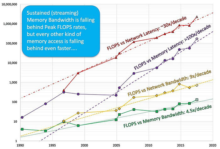
Figure 3. System latency over time compared to system bandwidth 4
In a way this is unsurprising. The world has never been more reliant on computer and computer networks as they become more and more a part of every aspect of our lives — in many ways for the better — driving improvements in efficiency, automation, optimization, connection, communication, and convenience to the benefit of humanity’s collective wellbeing. Data and the resources to process and move that data are a natural consequence. Now, society generates an average of over 328-million terabytes of data each day and in the process requires a total of more than 190 TWh per year 5, 6. In fact, by 2030, it is projected almost 20% of the world’s energy will be devoted to information and communications technology. In many ways innovations in processing have kept pace to face the challenges of increased data needs, but just as Dr. Miller quipped, bandwidth has now become a new and critical bottleneck. We may be able to process massive amounts of data — though admittedly we will always be pushing for more, but it’s far from trivial to move that data to where you may need it.
Compute power is improving much faster than memory and networks, leading to latency and bandwidth falling significantly behind processor performance — in other words memory and network connection (i.e., data movement) is becoming a critical bottleneck.
Current Challenges & Future Vision
For the vast majority of cases, the fundamentals of what makes up network connectivity is electricity, and naturally the mainstay of electrical infrastructure is the overwhelmingly pervasive copper that serves as its backbone. Today, this represents a cheap, mature, and effective network solution; however, electrical cables substantially degrade high-speed electrical signals, limiting the product of bit rate times distance to about 100 Gbps x meter for reasonable power consumption, density, and latency (e.g., 100 Gbps over 1 meter of cable, or 200 Gbps over ½ meter of cable). Optical fibers stretch that product to much beyond 100 Tbps x meter (e.g., 100 Gbps and beyond over 1,000 m of fiber). Hence, the higher per-lane I/O speeds become and the larger ML/AI clusters grow, the more critical is the transition from electronics to optics I/O. Figure 4
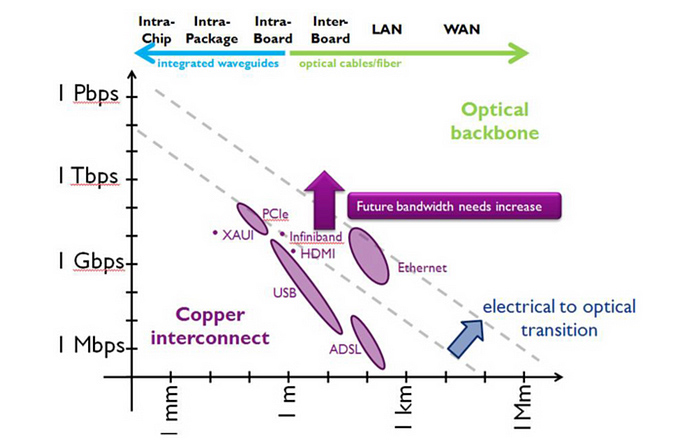
Figure 4. Bandwidth by distance applications requirements for short distance communication link 7
Advanced AI/ML training engines ask for hundreds of Tbps of full-duplex interconnect rates with edge I/O densities in the Tbps/mm range, exceeding the I/O needs of the latest generation of Ethernet switches. Meeting these high-chip escape densities, at low power and low latency, is key to enabling the viability of massive ML/AI clusters. The power and chip real estate required to drive and equalize high-speed electrical signals increases with their electrical reach. Hence, electrical fan-out must be avoided and a conversion from electrical to optical signals must happen as close to the ASIC as possible and at an I/O edge density that matches that of the ASIC 8 Figure 5.
Figure 5. Historical and potential future pathway of interconnection technologies.
The data center market is poised for remarkable growth with projections estimating a valuation of $1.6 trillion by 2027, and a serviceable available market (SAM) exceeding $3 billion. This robust expansion is fueled by the relentless surge in data consumption, the proliferation of digital technologies, and the increasing reliance on cloud services across various industries.
We identified the following technical metrics for a “King of the Hill” solution:
Performance: High speed to terabit per second (Tbps) range, high bandwidth density at Tbps/mm range, low latency, and reliable in wider temperature range
Power: High energy efficiency (order of magnitude better than copper)
Cost: Competitive link cost, matured-manufacturing process that can achieve good yield in mass production
Scalability: Integrate into chiplet architecture and compliance with standards such as Universal Chiplet Interconnect Express (UCIe), etc.
In addition, to succeed in the space there were so key business indicators that we felt should likely exist if such an endeavor was to succeed:
- Strong technical team and extensive industry experience in commercializing technology in this space
- Close partnership with major strategic customers and strong ecosystem engagement
- Deep-pocketed credible investors that understand this space well and have track record.
Nubis Communications: Paving the Way for Photonic Interconnection
TDK Ventures started its deep exploration in silicon photonics in 2021. In the past two years, we have already reviewed over 200 companies in optical communication and optical sensing space.
Nubis Communications emerged from the stealth mode in February 2023, unveiling a 1.6 Tbps optical engine enriched with integrated modulator drivers and transimpedance amplifiers. This quickly caught our attention as it sets a new bar for power efficiency and bandwidth density in silicon photonics Figure 6. Delivering a 16 x 112 Gbps = 1.6 Tbps link, its product demonstrated the industry’s highest power efficiency (<4 pJ/bit) and flaunting an impressive bandwidth density of up to 1 Tbps/mm in the category. The linear optics architecture allows Nubis’ engine to be directly driven by the host processor SerDes, therefore offering compelling power saving. The enterprise blends innovation in photonics, electronics, packaging, and manufacturing to orchestrate optical I/O products that are denser, more scalable, and more energy efficient compared to existing solutions. The team is a conglomerate of intellects led by Dr. Peter Winzer, a globally recognized technical maestro in the field. Notable entities like Matrix Partners, GV, and Imec.Xpand have been backing the development of this ground-break innovation.
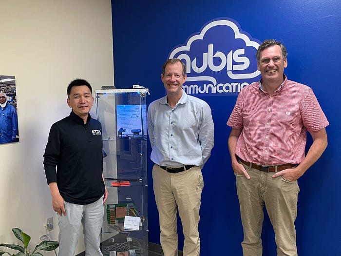
Figure 6. TDK Ventures visited Nubis office in New Jersey.
TDK Ventures conducted a thorough due diligence along with trusted partners such as Ericsson Ventures, Weili Dai and Sehat Sutardja, co-founders of Marvell Technology, who shared the vision and commitment to advancing the frontiers of optical technology. We conducted detailed lab testing on the chip, which confirmed the superior performance. We interviewed multiple customers and ecosystem partners, including high performance computing players, data center hyperscalers, data-communication solution providers, foundry-service providers. All spoke highly of the startup. Together, we concluded the Nubis’ King of the Hill status.
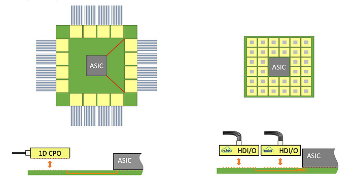
Figure 7. (a) Conventional beachfront-limited 1D CPO; (b) Scalable multi-row tiled HDI/O enabling 100-Tbps ML/AI I/O without the need for WDM.
The cutting-edge Nubis Optical Engine platform is the technology’s core, and with a compact millimeter footprint offers a solution scalable across applications. It successfully demonstrated a link that reaches 1.6 Tbps (16×112 Gbps) full-duplex throughput and an edge-escape density in the Tbps/mm range. Figure 7 compares the conventional co-packaged optics (CPO) modules using the one-dimensional (1D) photonic chip edge to escape optical fibers with Nubis’ linear-drive silicon photonics together with a novel 2D fiber escape. This allows a single-reticle ASIC to escape 100+ Tbps of aggregate I/O traffic at 100 Gbps/lane without the need to resort to Wavelength Division Multiplexing (WDM) 8.
References
1 Developments in optical computers: David Miller of AT&T Bell Labs, Holmdel Talks to Jo Ann McDonald, Euro III-Vs Review, Volume 3, Issue 3, Pages 34–37, ISSN 0959–3527. 1990.
2 What Is Moore’s Law and Is It Still Relevant in 2023? Make Use Of. Sieber, Tina. 2022, Mar 15.
3 Transistor count. 2023, September 24.
4 STREAM benchmark author McCalpin traces system balance trends. Trader, T., 2016, November 13.
5 Amount of data created daily. 2023.
6 Energy demand data centers globally by type 2021. 2020, March 25.
7 Polymer optical waveguide-based bi-directional optical bus architecture for high-speed optical backplane. Zhang, Xingyu, Et al. Proceedings of SPIE — The International Society for Optical Engineering. February 2012.
8 Ultra-Dense and Ultra-Low Power 16×112-Gbps Linear-Drive Silicon Photonics for ML/AI. OCP Global Summit. Peter Winzer, 2023.
9 Consumption linked to ICTs. 2018.